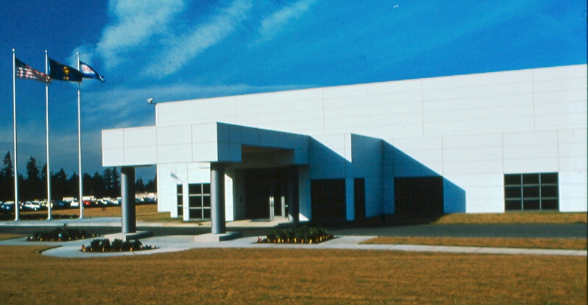
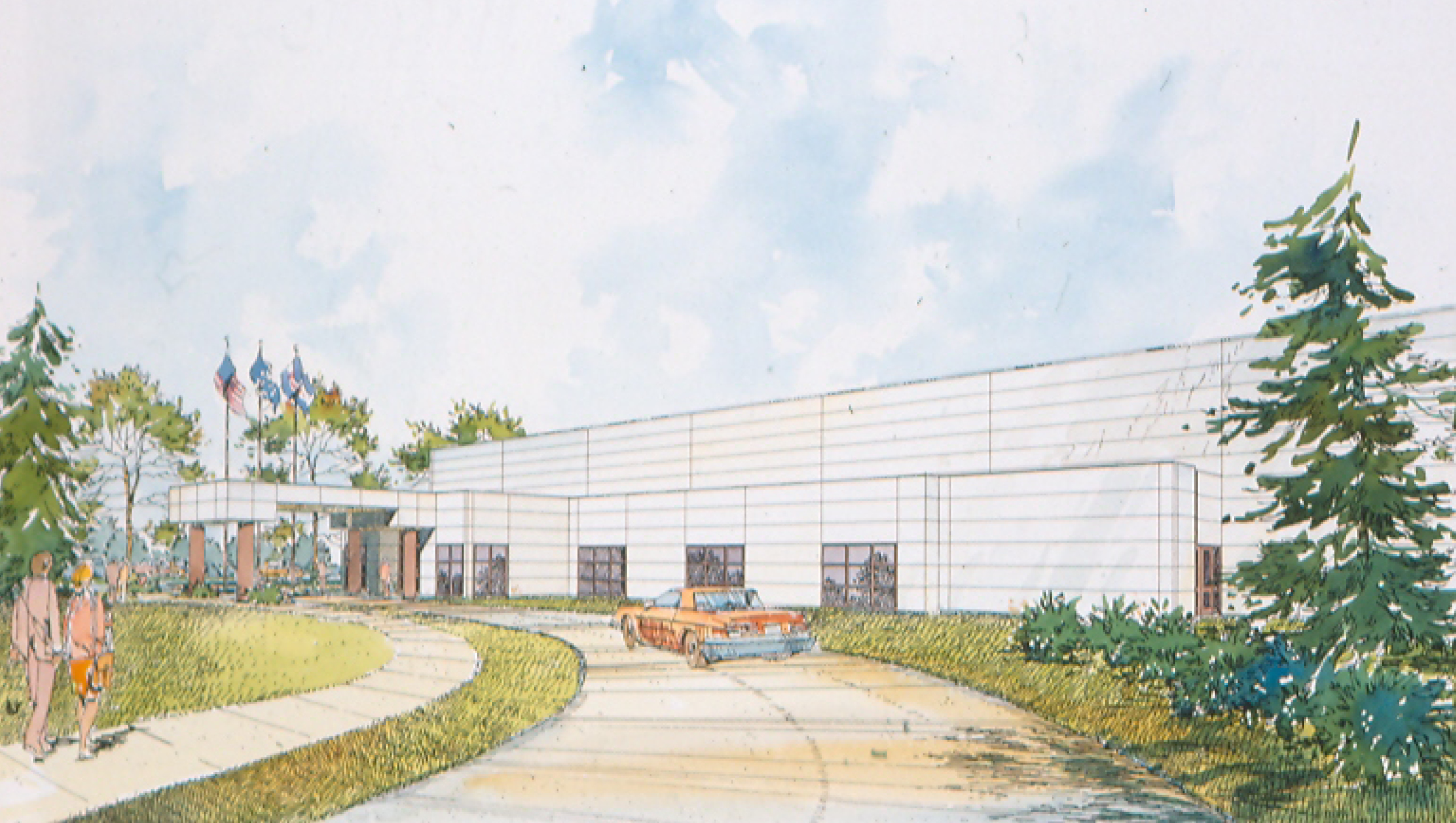
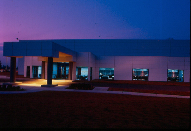
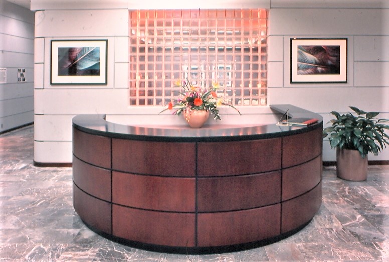
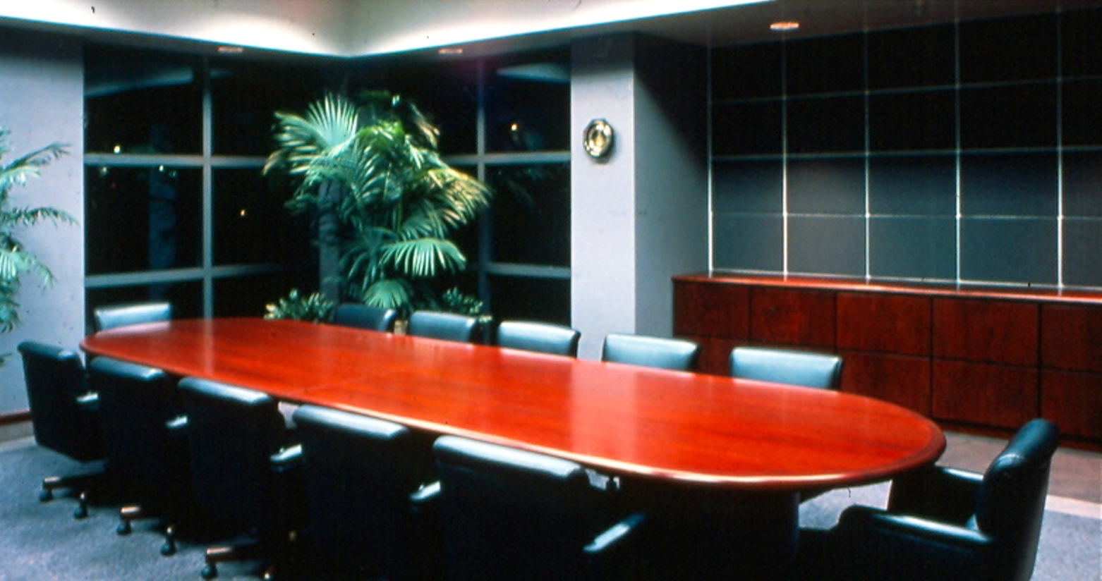
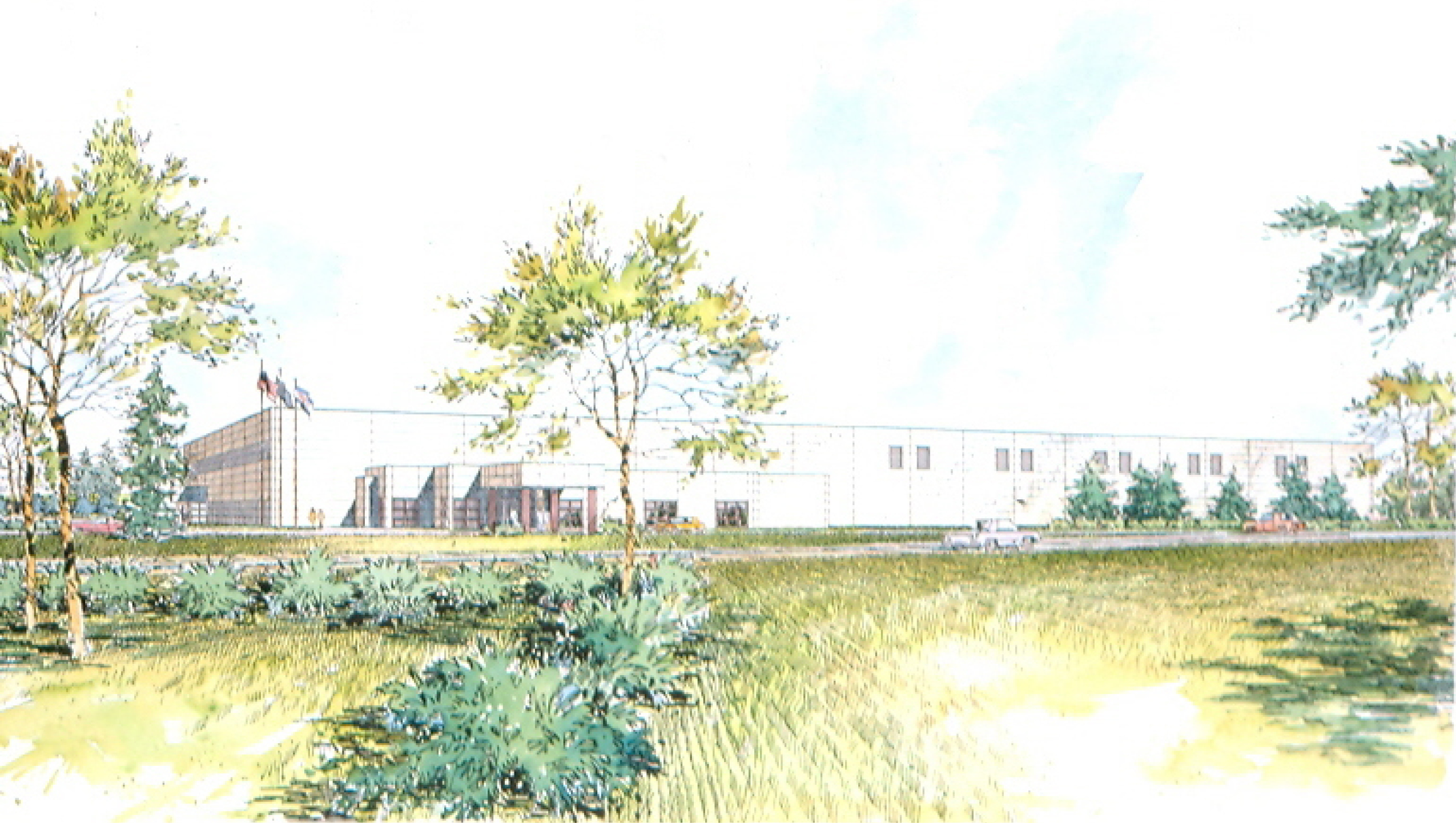
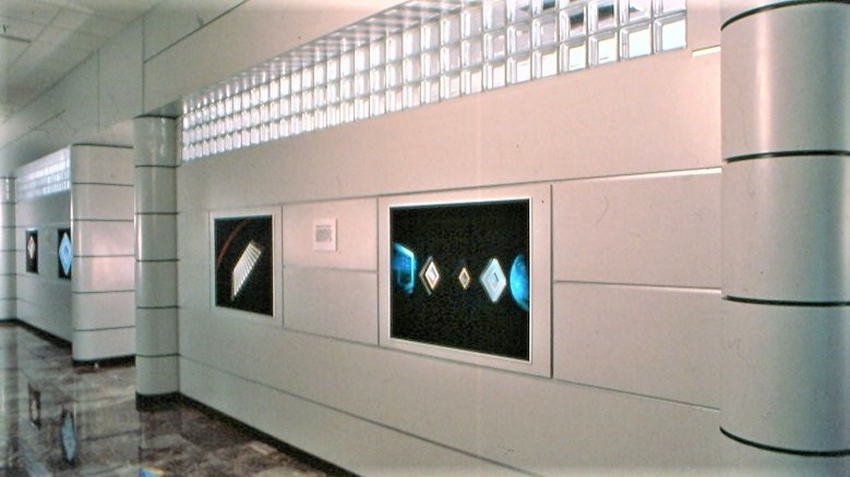
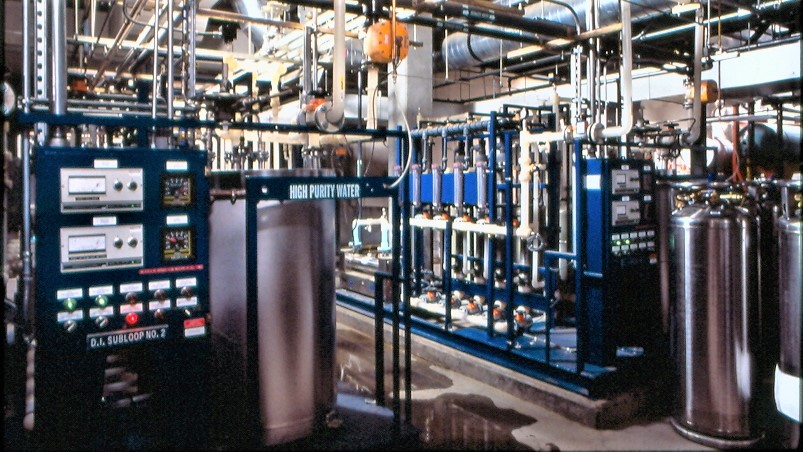
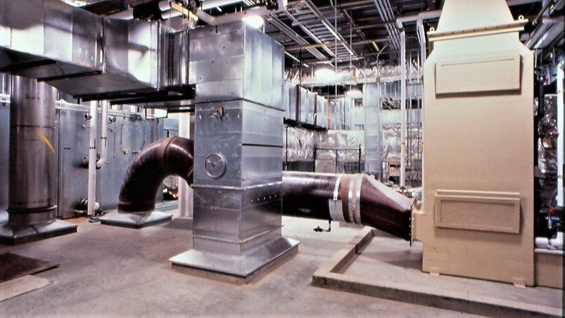
Fujitsu Micro Electronics, Inc. in Gresham Oregon, David W. Lewis, AIA (President, Context Design Group, PLLC) was the Project Architect on this project while working with CRSS, Inc. The project is comprised of very complicated Architectural & Structural Systems to support the H-3 Occupancy Use. The facility incorporates sophisticated “State of the Art” Mechanical & Electrical Systems providing for a series of Cleanrooms ranging in Levels from 100,000 to 10. The project incorporated the use of HPM corridors for transporting and delivering hazardous materials to production areas. Project was completed as a Fast-Track Design / Build project in a total of 14 Months from beginning of Conceptual Design to starting up of the Wafer Fabrication Production Facility.